|
Semiconductor fabrication plant

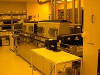
In the microelectronics industry, a semiconductor fabrication plant, also called a fab or a foundry, is a factory where integrated circuits (ICs) are manufactured.[1] The cleanroom is where all fabrication takes place and contains the machinery for integrated circuit production such as steppers and/or scanners for photolithography, etching, cleaning, and doping. All these devices are extremely precise and thus extremely expensive. Prices for pieces of equipment for the processing of 300 mm wafers range to upwards of $4,000,000 each with a few pieces of equipment reaching as high as $340,000,000 (e.g. EUV scanners). A typical fab will have several hundred equipment items. Semiconductor fabrication requires many expensive devices. Estimates put the cost of building a new fab at over one billion U.S. dollars with values as high as $3–4 billion not being uncommon. For example, TSMC invested $9.3 billion in its Fab15 in Taiwan.[2] The same company estimations suggest that their future fab might cost $20 billion.[3] A foundry model emerged in the 1990s: Companies owning fabs that produced their own designs were known as integrated device manufacturers (IDMs). Companies that outsourced manufacturing of their designs were termed fabless semiconductor companies. Those foundries which did not create their own designs were called pure-play semiconductor foundries.[4] In the cleanroom, the environment is controlled to eliminate all dust, since even a single speck can ruin a microcircuit, which has nanoscale features much smaller than dust particles. The clean room must also be damped against vibration to enable nanometer-scale alignment of photolithography machines and must be kept within narrow bands of temperature and humidity. Vibration control may be achieved by using deep piles in the cleanroom's foundation that anchor the cleanroom to the bedrock, careful selection of the construction site, and/or using vibration dampers. Controlling temperature and humidity is critical for minimizing static electricity. Corona discharge sources can also be used to reduce static electricity. Often, a fab will be constructed in the following manner (from top to bottom): the roof, which may contain air handling equipment that draws, purifies and cools outside air, an air plenum for distributing the air to several floor-mounted fan filter units, which are also part of the cleanroom's ceiling, the cleanroom itself, which may or may not have more than one story, [5] a return air plenum, the clean subfab that may contain support equipment for the machines in the cleanroom such as chemical delivery, purification, recycling and destruction systems, and the ground floor, that may contain electrical equipment. Fabs also often have some office space.  HistoryTypically an advance in chip-making technology requires a completely new fab to be built. In the past, the equipment to outfit a fab was not very expensive and there were a huge number of smaller fabs producing chips in small quantities. However, the cost of the most up-to-date equipment has since grown to the point where a new fab can cost several billion dollars. Another side effect of the cost has been the challenge to make use of older fabs. For many companies these older fabs are useful for producing designs for unique markets, such as embedded processors, flash memory, and microcontrollers. However, for companies with more limited product lines, it is often best to either rent out the fab, or close it entirely. This is due to the tendency of the cost of upgrading an existing fab to produce devices requiring newer technology to exceed the cost of a completely new fab. There has been a trend to produce ever larger wafers, so each process step is being performed on more and more chips at once. The goal is to spread production costs (chemicals, fab time) over a larger number of saleable chips. It is impossible (or at least impracticable) to retrofit machinery to handle larger wafers. This is not to say that foundries using smaller wafers are necessarily obsolete; older foundries can be cheaper to operate, have higher yields for simple chips and still be productive. The industry was aiming to move from the state-of-the-art wafer size 300 mm (12 in) to 450 mm by 2018.[6] In March 2014, Intel expected 450 mm deployment by 2020.[7] But in 2016, corresponding joint research efforts were stopped.[8] Additionally, there is a large push to completely automate the production of semiconductor chips from beginning to end. This is often referred to as the "lights-out fab" concept. The International Sematech Manufacturing Initiative (ISMI), an extension of the US consortium SEMATECH, is sponsoring the "300 mm Prime" initiative. An important goal of this initiative is to enable fabs to produce greater quantities of smaller chips as a response to shorter lifecycles seen in consumer electronics. The logic is that such a fab can produce smaller lots more easily and can efficiently switch its production to supply chips for a variety of new electronic devices. Another important goal is to reduce the waiting time between processing steps.[9][10] See also
Notes
References
Further reading
|
||||||