|
Semiconductor device modeling
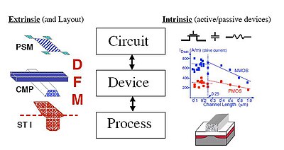
 Semiconductor device modeling creates models for the behavior of semiconductor devices based on fundamental physics, such as the doping profiles of the devices. It may also include the creation of compact models (such as the well known SPICE transistor models), which try to capture the electrical behavior of such devices but do not generally derive them from the underlying physics. Normally it starts from the output of a semiconductor process simulation. Introduction The figure to the right provides a simplified conceptual view of "the big picture". This figure shows two inverter stages and the resulting input-output voltage-time plot of the circuit. From the digital systems point of view the key parameters of interest are: timing delays, switching power, leakage current and cross-coupling (crosstalk) with other blocks. The voltage levels and transition speed are also of concern. The figure also shows schematically the importance of Ion versus Ioff, which in turn is related to drive-current (and mobility) for the "on" device and several leakage paths for the "off" devices. Not shown explicitly in the figure are the capacitances—both intrinsic and parasitic—that affect dynamic performance. The power scaling which is now a major driving force in the industry is reflected in the simplified equation shown in the figure—critical parameters are capacitance, power supply and clocking frequency. Key parameters that relate device behavior to system performance include the threshold voltage, driving current and subthreshold characteristics. It is the confluence of system performance issues with the underlying technology and device design variables that results in the ongoing scaling laws that we now codify as Moore's law. Device modelingThe physics and modeling of devices in integrated circuits is dominated by MOS and bipolar transistor modeling. However, other devices are important, such as memory devices, that have rather different modeling requirements. There are of course also issues of reliability engineering—for example, electro-static discharge (ESD) protection circuits and devices—where substrate and parasitic devices are of pivotal importance. These effects and modeling are not considered by most device modeling programs; the interested reader is referred to several excellent monographs in the area of ESD and I/O modeling.[1][2][3] Physics driven vs. compact models Physics driven device modeling is intended to be accurate, but it is not fast enough for higher level tools, including circuit simulators such as SPICE. Therefore, circuit simulators normally use more empirical models (often called compact models) that do not directly model the underlying physics. For example, inversion-layer mobility modeling, or the modeling of mobility and its dependence on physical parameters, ambient and operating conditions is an important topic both for TCAD (technology computer aided design) physical models and for circuit-level compact models. However, it is not accurately modeled from first principles, and so resort is taken to fitting experimental data. For mobility modeling at the physical level the electrical variables are the various scattering mechanisms, carrier densities, and local potentials and fields, including their technology and ambient dependencies. By contrast, at the circuit-level, models parameterize the effects in terms of terminal voltages and empirical scattering parameters. The two representations can be compared, but it is unclear in many cases how the experimental data is to be interpreted in terms of more microscopic behavior. HistoryThe evolution of technology computer-aided design (TCAD)—the synergistic combination of process, device and circuit simulation and modeling tools—finds its roots in bipolar technology, starting in the late 1960s, and the challenges of junction isolated, double-and triple-diffused transistors. These devices and technology were the basis of the first integrated circuits; nonetheless, many of the scaling issues and underlying physical effects are integral to IC design, even after four decades of IC development. With these early generations of IC, process variability and parametric yield were an issue—a theme that will reemerge as a controlling factor in future IC technology as well. Process control issues—both for the intrinsic devices and all the associated parasitics—presented formidable challenges and mandated the development of a range of advanced physical models for process and device simulation. Starting in the late 1960s and into the 1970s, the modeling approaches exploited were dominantly one- and two-dimensional simulators. While TCAD in these early generations showed exciting promise in addressing the physics-oriented challenges of bipolar technology, the superior scalability and power consumption of MOS technology revolutionized the IC industry. By the mid-1980s, CMOS became the dominant driver for integrated electronics. Nonetheless, these early TCAD developments[4][5] set the stage for their growth and broad deployment as an essential toolset that has leveraged technology development through the VLSI and ULSI eras which are now the mainstream. IC development for more than a quarter-century has been dominated by the MOS technology. In the 1970s and 1980s NMOS was favored owing to speed and area advantages, coupled with technology limitations and concerns related to isolation, parasitic effects and process complexity. During that era of NMOS-dominated LSI and the emergence of VLSI, the fundamental scaling laws of MOS technology were codified and broadly applied.[6] It was also during this period that TCAD reached maturity in terms of realizing robust process modeling (primarily one-dimensional) which then became an integral technology design tool, used universally across the industry.[7] At the same time device simulation, dominantly two-dimensional owing to the nature of MOS devices, became the work-horse of technologists in the design and scaling of devices.[8][9] The transition from NMOS to CMOS technology resulted in the necessity of tightly coupled and fully 2D simulators for process and device simulations. This third generation of TCAD tools became critical to address the full complexity of twin-well CMOS technology (see Figure 3a), including issues of design rules and parasitic effects such as latchup.[10][11] An abbreviated perspective of this period, through the mid-1980s, is given in;[12] and from the point of view of how TCAD tools were used in the design process, see.[13] See alsoReferences
|