|
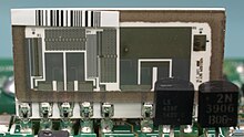
Laser trimmingLaser trimming is the manufacturing process of using a laser to adjust the operating parameters of an electronic circuit.  One of the most common applications uses a laser to burn away small portions of resistors, raising their resistance value. The burning operation can be conducted while the circuit is being tested by automatic test equipment, leading to optimum final values for the resistor(s) in the circuit. The resistance value of a film resistor is defined by its geometric dimensions (length, width, height) and the resistor material. A lateral cut in the resistor material by the laser narrows or lengthens the current flow path and increases the resistance value. The same effect is obtained whether the laser changes a thick-film or a thin-film resistor on a ceramic substrate or an surface-mount resistor. The surface-mount resistor is produced with the same technology and may be laser trimmed as well. Trimmable chip capacitors are built up as multilayer plate capacitors. Vaporizing part of the top layer with a laser decreases the capacitance by reducing the area of the top electrode. Passive trim is the adjustment of a resistor to a given value. If the trimming adjusts the whole circuit output such as output voltage, frequency, or switching threshold, this is called active trim. During the trim process, the corresponding parameter is measured continuously and compared to the programmed nominal value. The laser stops automatically when the value reaches the nominal value. Trimming LTCC resistances in a pressure chamberOne type of passive trimmer uses a pressure chamber to enable resistor trimming in a single run. The LTCC boards are contacted by test probes on the assembly side and trimmed with a laser beam from the resistor side. This trimming method requires no contact points between the resistances, because the fine pitch adapter contacts the component on the opposite side of where the trimming occurs. Therefore, the LTCC can be arranged more compactly and less expensively.  Function mode:
Advantages of this method:
Trimming potentiometersOften designers use potentiometers, which are adjusted during end testing until the desired function of the circuit is reached. In many applications, the end user of the product would prefer not to have potentiometers, as they can drift, be mis-adjusted or develop noise. Therefore, manufacturers determine the needed resistance or capacitance values by measurement and calculation methods and afterwards solder the suitable component into the final PCB; this approach is called "Select on Test" (SOT) and is quite labor-intensive. It is simpler to substitute the potentiometer or the SOT part with a trimmable chip resistor or chip capacitor, and the potentiometer adjusting screwdriver is replaced by the laser trimming. The achieved accuracy can be higher, the procedure can be automated, and the long-term stability is better than with potentiometers and at least as good as with SOT components. Often the laser for active trimming can be integrated in existing measurement systems by the manufacturer. Program from digital logic circuitsA similar approach can be used to program digital logic circuits. In this case, fuses are blown by the laser, enabling or disabling various logic circuits. An example of this is the IBM POWER4 microprocessor where the chip contains five banks of cache memory but only requires four banks for full operation. During testing, each cache bank is exercised. If a defect is found in one bank, that bank can be disabled by blowing its programming fuse. This built-in redundancy allows higher chip yields than would be possible if all cache banks had to be perfect in every chip. If no bank is defective, a fuse can be blown arbitrarily, leaving just four banks. |